FERRUM WANDLA I/V CONVERTER
in general
I/V converters in general
Current output is typical in high-performance audio DACs. However, line input voltage signals are the standard for audio amplifiers, so a current-to-voltage (I/V) converter is required in the signal path. The simplest example of I/V converter is a resistor. Current flow results in a voltage drop across the resistor; this voltage is equal to the current multiplied by the resistance. Although a resistor is a simple and effective I/V converter, it is rarely used in designs with current output DACs. For many DAC’s, a low impedance load is a prerequisite for optimal operation. With the resistor-based I/V convertor, any increase in the desired output voltage requires a higher value resistor which is inconsistent with this low impedance load requirement. Therefore, active solutions are used to fulfill high output voltage and low input impedance requirements.
This active solution is called a transimpedance amplifier, and its simplified schematic is shown in Fig. 1. An operational amplifier uses negative feedback to minimize the voltage difference between the positive and negative inputs of amplifier U1 (ideally to zero). Therefore, current source I1 (DAC output) sees ground potential and low impedance to ground. This effect is called virtual ground. At the same time, current (I) flows through resistor R1, so there is I/V conversion as in the simple resistor circuit. However, the output signal is out of phase with the input current. This topology provides a low input impedance to the amplifier, regardless of the value of resistor R1, which is a significant benefit. These characteristics of transimpedance amplifiers are the reason for their common use as I/V converters in current output DACs.
ESS9038PRO current output stage
In the case of ES9038PRO, its current output stage is quite challenging. It has a strikingly high output current, and if its output channels are paralleled for error averaging, the total current is even higher. This combined current is so high most operational amplifiers used in I/V converters will start to distort the signal. Therefore, a typical solution incorporates separate I/V converters for each output channel and combines the outputs of the multiple I/V converters. This is shown in Fig. 2.
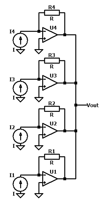
When the DACs’ outputs are combined after the I/V stages, the current flowing through each I/V converter is smaller; therefore, the distortion level is lower. There is still error averaging, as it would be with directly paralleled current outputs (I1, I2, I3, I4), but now the errors are averaged on the voltage output of I/V converters. However, there is an additional source of error in this configuration. Each I/V converter has a resistor (R1, R2, R3, R4). In theory, they have the same value, but in practice, there is tolerance to the value of this resistance. Deviation from the nominal value of this resistance will change the gain of each I/V converter and will affect the final averaging of errors from each ESS DAC current output (I1, I2, I3, I4). Therefore, in Wandla, we adopted a different I/V converter topology.
Wandla I/V converter
In Wandla, instead of employing multiple I/V converters in each output channel, we designed a composite amplifier to drive the combined current of paralleled ESS DAC outputs without additional distortion. This solution is shown in Fig. 3.
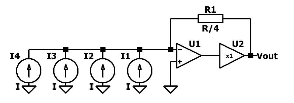
ES9038PRO current outputs (I1, I2, I3, I4) are directly paralleled, and then the composite amplifier converts the total current to voltage. This amplifier consists of two separate ICs, and the value of resistance R1 in the feedback loop is now one-fourth of that used in the typical circuit because the current flowing through the I/V converter is four times higher.
U1 is a fast, low-noise current feedback operational amplifier (CFB). CFB operational amplifiers are beneficial in transimpedance amplifiers because, on their inverting input (-), they have low impedance, which keeps the impedance low on the input of transimpedance amplifier even at high frequencies, where the feedback loop is not able to keep the impedance low. This is important because the output current of ESS DAC still has the spectrum of signal components of Delta-Sigma modulation, which can have a bandwidth over 10 MHz. Of course, those frequencies are attenuated by the antialiasing filter after the I/V converter. Still, a transimpedance amplifier that cannot properly sink those fast currents will add errors to the Delta-Sigma modulation signal shape, distorting the signal in the audio band.
U2 is a fast voltage follower that can provide a higher current than the amplifier U1. It is a current buffer with a high input impedance; therefore, U1 is less loaded, and the distortion of the composite amplifier consisting of U1 and U2 is much lower. For reference, when using the same current feedback operational amplifier U1, the conventional configuration (with four I/V converters per channel) had over 10 db higher THD than our composite amplifier from Fig. 3 (with only one I/V) comprised of U1 and U2 in a feedback loop.
It’s a common refrain: “All ESS DACs sound the same”, or “all ESS-based DACs have the Sabre sound signature”. Each aspect of Wandla’s unique I/V converter topology may seem minor on its own, but together they create astonishingly transparent and effortless sound reproduction that definitively leaves the “Sabre sound signature” behind.